Scientific staff
- Y. André (Assistant Professor HDR, UCA, CNU 28)
- G. Avit (Engineer, UCA)
- E. Gil (Professor, UCA, CNU 28)
- A. Trassoudaine (Professor, UCA, CNU 28)
- E. Chereau (PhD)
- E. Semlali (PhD)
What is HVPE?
Institut Pascal is the only laboratory in the world developing research on Hydride Vapor Phase Epitaxy or HVPE for the growth of both III-V (Ga,In)-(As,P) and III-N (Ga,In)-N semiconductor (nano)structures.
HVPE implements high mass inputs of hydride VH3 and NH3, and chlorinated IIICl gas precursors of which decomposition frequency is fast.
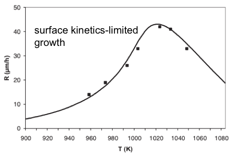
Because of the fast precursor decomposition, there is no kinetic delay so that we observe immediate reactivity to an increase of the supersaturation of the vapor phase towards return to equilibrium which produces the solid. The variation of growth rate as a function of temperature shows the typical bell curve, related to growth controlled by thermodynamics and surface kinetics.
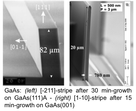
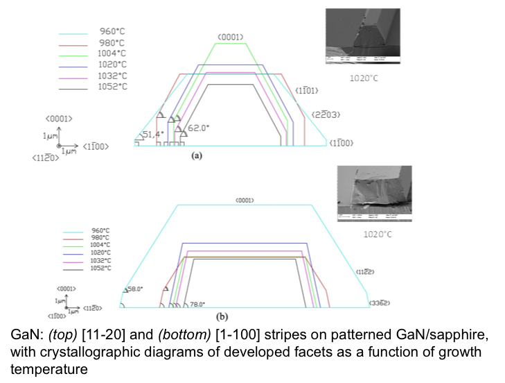
High growth anisotropy towards the controlled shaping of structures
The growth rate can be modulated by simply varying the mass input rate of the reactants. It is then possible to fully take advantage of the growth anisotropy of III-(V,N) crystals as a wide range of condensation rates can be set from 3 to more than 100 µm/h as a function of the temperature, the vapor phase composition, for each face of the crystals.
|
|
|
|
Selected papers
• E. Gil et al., Hydride VPE for current III-V and nitride semiconductor compound issues, Handbook of Crystal Growth, Vol. III, Second Edition, Elsevier, Chapter 2, 51 (2015)
• F. Reveret et al., Spatially resolved optical control of GaN grown by selective area hydride vapor phase epitaxy, Journal of Crystal Growth 421, 27 (2015)
• E. Gil et al., Record high-aspect-ratio GaAs nano-grating lines grown by Hydride Vapor Phase Epitaxy (HVPE), J. Crystal Growth 380, 93 (2013)
• Y. Andre et al., Demonstration of crystal-vapor equilibrium leading to a growth blockade of GaN during selective area growth, Journal of Crystal Growth 354, 135 (2012)
• O. Chelda-Gourmala et al., Complete HVPE experimental investigations: cartography of SAG GaN towards quasi-substrates or nanostructures, Journal of Crystal Growth 312, 1899 (2010)
HVPE for fast growth of ultra-long nanowires
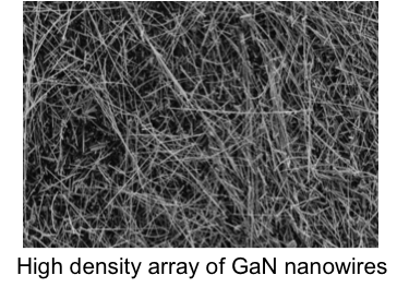
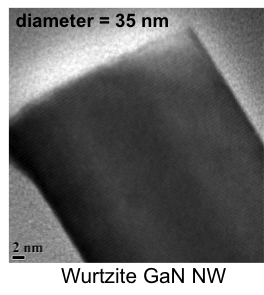
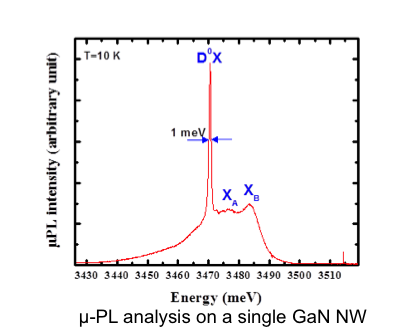
Metal (Au or Ni-Au)-assisted Vapor Liquid Solid (VLS) growth in the HVPE environment produces very long polytypism-free nanowires (NWs) in short process times, with elongation rates ranging from 100 to 200 µm/h, with constant diameter and constant phase.
|
|
 |
 |

HVPE demonstrates state of the art pure cubic zincblende phase in record 5 nm radius-GaAs NWs.
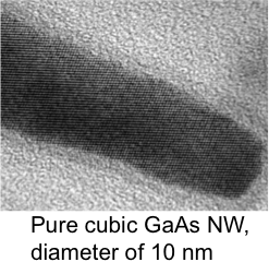 |
Why? Pure axial growth of the nanowires is favored as a result of the direct supply of the precursors through the catalyst droplets. High mass input of precursors yields high Ga concentration in the liquid droplet, decreasing the surface energy. Nucleation then takes place at the liquid-solid center line, which generates a cubic zincblende phase whatever the radius of the nanowire is. |
Selected papers
• G. Avit et al., Ultralong and defect-free GaN nanowires by the HVPE process, Nano Letters 14, 559 (2014)
• E. Gil et al., Record pure zincblende phase in GaAs nanowires down to 5 nm in radius, Nano Letters 14, 3938 (2014)
• G. Avit et al., Catalyst-assisted Hydride Vapor Phase Epitaxy of GaN nanowires: exceptional length and constant rod like shape capability, Nanotechnology 23, 405601 (2012)
• M.R. Ramdani et al., Fast Growth Synthesis of GaAs Nanowires with Exceptional Length, Nano Letters 10, 1836 (2010)
HVPE for the growth of GaN nanorods on Si / hybrid MOVPE/ HVPE process
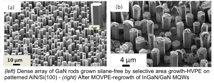
Dense arrays of GaN rods are grown by selective area HVPE growth on patterned AlN/Si (100). High aspect ratio rods are actually obtained without the use of silane or any other gaseous precursors except GaCl and NH3. First demonstration of MOVPE regrowth of InGaN/GaN multi-quantum wells (MQWs) shells on HVPE-GaN cores for LED devices.
Selected papers
• G. Avit et al., GaN rods grown on Si by SAG-HVPE towards GaN HVPE/InGaN MOVPE core/shell structures, Crystal Growth and Design 16, 2509 (2016)
• A. Trassoudaine et al., Spontaneous formation of GaN/AlN core-shell nanowires on sapphire by HVPE, J. Crystal Growth 454, 1 (2016)
HVPE growth of nanowires: whats to come?
• Self-catalyzed NW growth: to be brought online soon.
Selected papers
• Z. Dong et al., Self-catalyzed GaAs nanowires on silicon by HVPE, Nanotechnology 28, 125602 (2017)
• V.G. Dubrovskii et al., Nucleation and initial radius of self-catalyzed III-V nanowires, J. Crystal Growth 459, 194 (2017)
• InGaN NW growth with tunable In composition: to be brought online soon.
Visit us within a few weeks!

Collaborations
• Pr. Hiroshi AMANO, Nobel Prize of Physics in 2014, Nagoya University (Japan). Honoris Causa Professor of Université Blaise Pascal and Université d'Auvergne in 2016. Collaboration on the project INSOLIUM, "InGaN nanowires-based solar cells on silicon substrate" funded by PRC CNRS-JSPS and the foundation of Université d'Auvergne.
• Pr. Vladimir DUBROVSKII, St Petersburg Academic University, IOFFE Physical Technical Institute of St Petersburg, ITMO University of St Petersburg. Regular invited Professor (Université Blaise Pascal / IMobS3 LabEx). Modelling of nanowire growth.
• ITMO St Petersburg (Russia) international collaboration contract. Nanowire growth.
• Group of partners from AURA Region: INAC CEA (Grenoble), Institut des Nanotechnologies (INL) (Lyon), Institut Néel (Grenoble). Involved in the ENNORA project (see below).
National and international projects
- The HVPE team is a partner of the French Laboratoire d’Excellence GaNeX (since 2012) which gathers the nitride French scientific community.
- Project ENNORA: Growth of semiconductor nanowires for energy. Structural and optical properties, electric transport. Funded by AURA Region (2017-2020).
- French project ANR “FIDEL” 2012-2015: InGaN Nanowires for Electroluminescent Diodes. Our team develops the growth of InGaN nanowires with controlled morphologies and optical properties. Collaborations: CEA/LETI-Grenoble and Institut Néel, Grenoble, France.
- French project ANR "SPINJECT" 2006-2009: Spin polarized tunneling from an optically excited GaAs tips. We have demonstrated the potential of the HVPE process to grow GaAs tips with controlled morphologies required for spin injection to be used for spin polarised scanning tunneling microscopy (collaboration: Ecole Polytechnique Palaiseau, Laboratoire PMC, France).
- European project PARSEM 2005-2009 (6e PCRDT CEE RTN): Interfacial phenomena at atomic resolution and multi-scale properties of novel III-V semiconductors. The HVPE process provided very thick GaN layers (0.5 mm) with record low dislocation density (<106 cm-2).


