


DreamCam is a modular smart camera constructed with the use of an FPGA like main processing board. The core of the camera is an Altera Cyclone-III EP3C120 associated with a CMOS imager and six private Ram blocks. The main novel feature of our work consists in proposing a new smart camera architecture and several modules (IP) to efficiently extract and sort the visual features in real time.
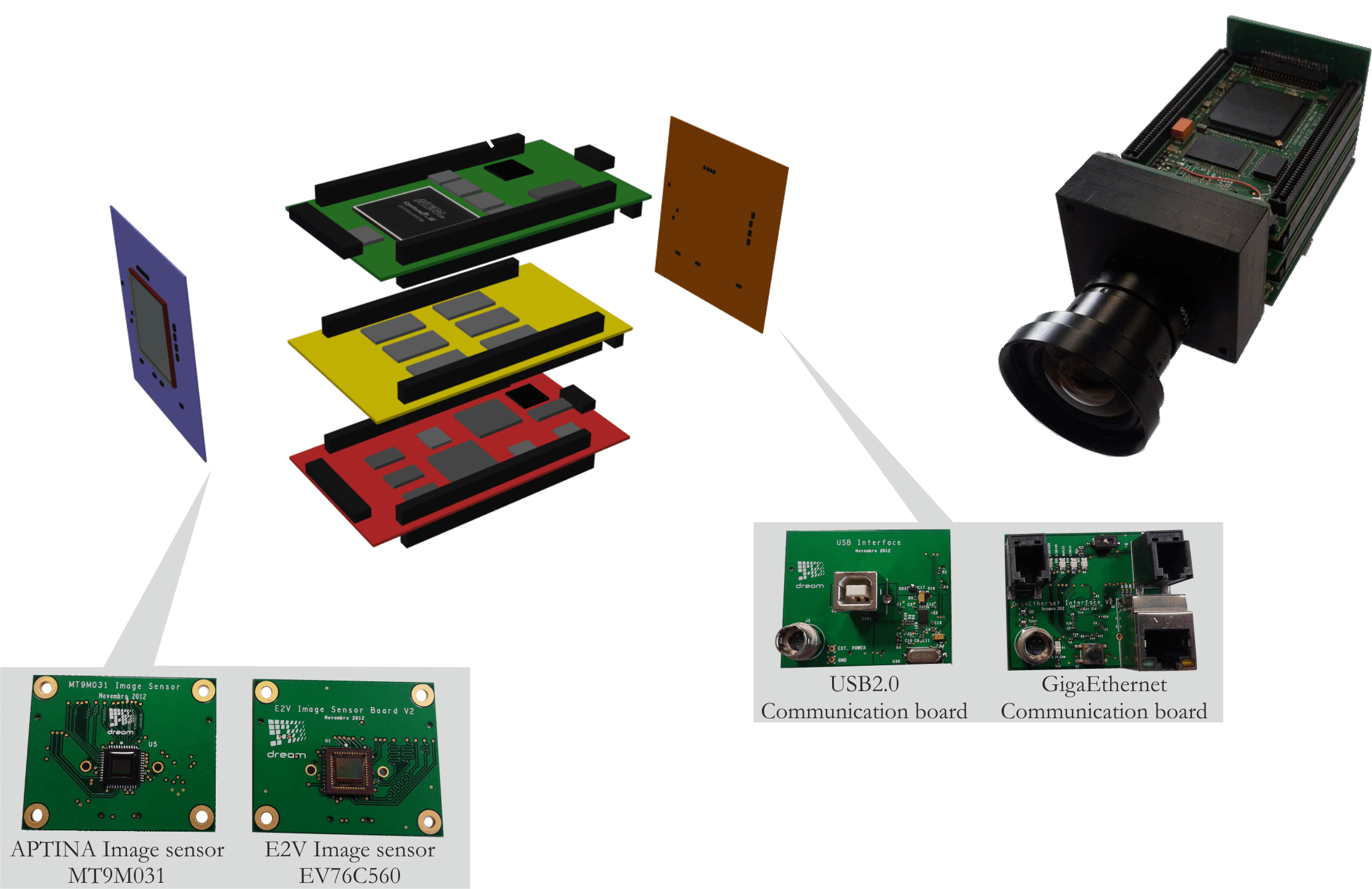
The architecture of the camera is constructed with five interconnected boards as shown in figure above. The core of this system is a FPGA which allows a high versatility. Thus, the image sensor board and the communication board can be easily replaced or updated in order to change the type of imager or the communication layer. Currently, we can propose two different image sensors and the ability to use a USB2.0 or Giga-Ethernet communication link.
Both developed image sensor boards are based on a similar electronic architecture.
This architecture can accept parallel differential or single-ended outputs from different kinds of image sensors. The image sensors used in this work are:
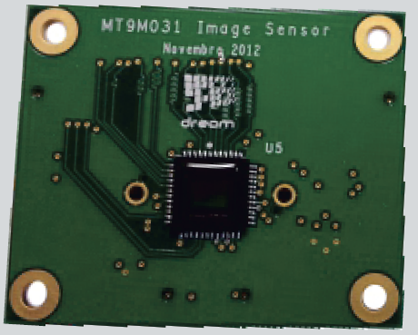
- MT9M031 imager: This 1.2-mega pixel (1280x960)CMOS image sensor is manufactured by Aptina. It can operate at 45 fps at full 1280x960 pixel resolution or at 60fps speed at 720pHD resolution (reduced FOV). The power consumption is 270mW in 720p60 mode. The dynamic range is 83.5dB - quite big for a global shutter sensor.
- EV76C560 imager: This is a 1.3-mega pixel (1280x1024) CMOS active pixel sensor dedicated to industrial vision features both rolling and global shutters. The pixel design offers excellent performance in low-light conditions with a high-readout speed of 60 fps in full resolution. Novel pixel integration/readout modes and embedded image pre-processing deliver superior
performance parameters, including a bi-frame wide dynamic range (> 100dB). Other on-chip pre-processing are included such as Image Histograms, Multi-ROI, Defective pixel correction,...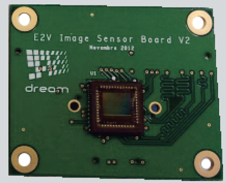
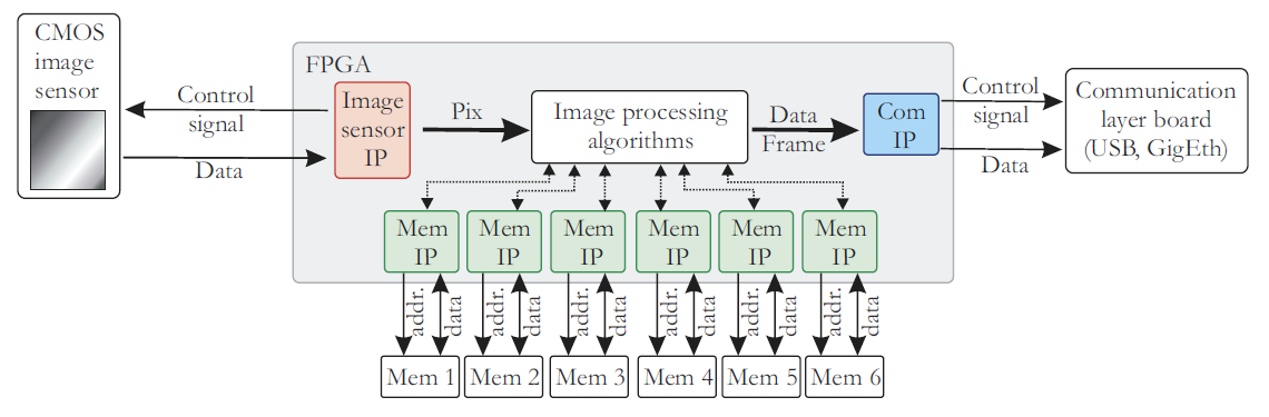
The internal FPGA design is to create a flexible interface between the sensing device board and the host computer. This is how the whole system is separated into two main parts:
- a software part which is basically a C++ code that retrieves the data that are in the USB packets sent from DreamCam
- a hardware part whtih differents part (IP):
- The first one controls the CMOS image sensor which is the Image sensor IP block
- The second manages communication between the host computer
- The Mem IP block is used when external memories are needed. Theses blocks control each memory by generating the appropriate input signal of the memory such as (Address Bus : A0-A19, Chip Enable signal : CE, Write Enable signal : WE, Output Enable signal : OE) and by receiving the data.
- Finally the Image processing algorithm block will contain the algorithm that we want to implement on FPGA
Internal FPGA design
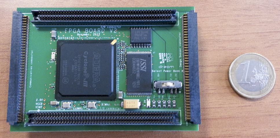
Global view of the FPGA Board
A typical demo (Harris point extraction)